

Loadport and alignment
Wafers and adapters enter the cell, align, and move into measurement or processing steps.
ATP is designed to bring wafer-adapter handling, loadports, alignment, robot and station movement, metrology positions, and process-data context into one configurable automation platform.
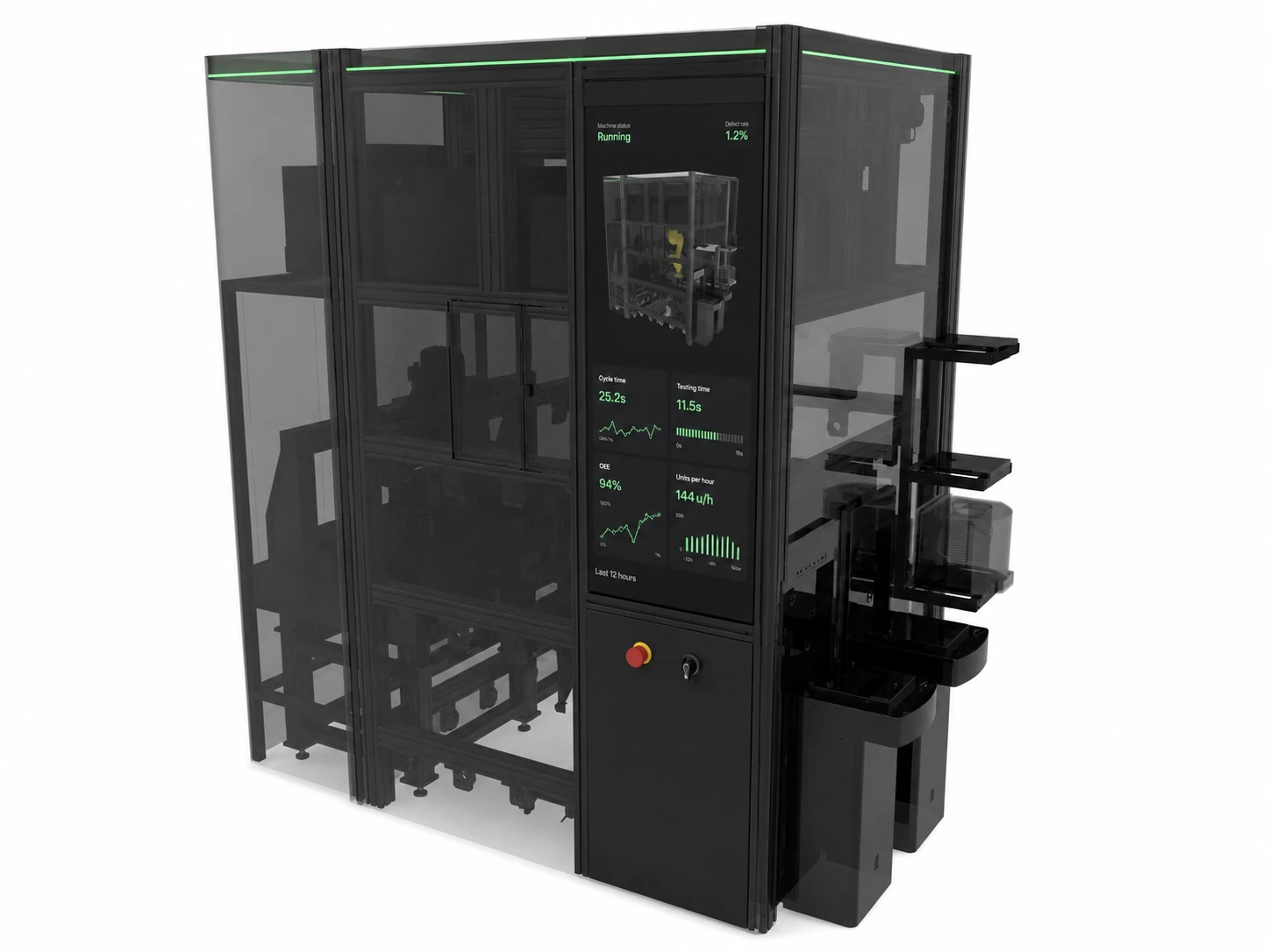
ATP connects wafer-adapter handling with measurement positions and process-data context, so teams can shape a workflow around a specific substrate, tool path, and measurement need.
Software options, status views, and factory interfaces can be scoped when the workflow needs them.
Platform architecture
ATP organizes loadport and alignment steps around a handling core, uses reusable adapters to bridge substrate sizes, places metrology options near the workflow, and connects process data for comparison across steps.
Wafers and adapters enter the cell, align, and move into measurement or processing steps.
Station layouts are matched to the handling, transfer, and sensor tasks required by the workflow.
Adapter insertion, substrate fixation, workflow routing, and removal are built around the selected adapter variant.
Measurement options can be placed around the handling layout when inline inspection is needed.
Sensitive instruments can use vibration-isolated foundations or decoupled module positions.
Status views, troubleshooting tools, and factory-interface needs are scoped to the workflow.
Platform capabilities
Places smaller substrates into reusable adapters, routes them through process or measurement steps, and removes them again.
Configured around loadports, wafer alignment, automated movement, and recipe-driven workflows.
Robot and station layouts can be matched to different handling or sensor tasks.
Measurement positions can be selected for optical inspection, spectral imaging, thickness, topography, wafer-shape checks, weighing, particle checks, or carrier-environment options.
Sensitive instruments can use vibration-isolated foundations or decoupled module positions.
Status views, troubleshooting tools, and factory interfaces are scoped to project needs.
Metrology module categories
Module categories are selected per project based on measurement goals, substrate handling, and integration constraints. Options include optical inspection, spectral imaging, thickness measurement, topography, wafer-shape checks, particle checks, weighing, and carrier-environment options.
Surface features and local defect context
Material contrast and process-state signals
Layer thickness and film-uniformity indicators
Surface profile, wafer bow, and deformation context
Contamination checks and model-comparison context
Mass-change checks and controlled carrier handling
Example application areas
Application fit depends on the target substrate, tool path, and measurement scope. ATP workflows can add inline data where better process visibility is needed.
Evaluate how smaller substrates move through existing equipment with adapter-based handling.
Add inline measurement context for model-comparison work.
Select optical, spectral, thickness, or topography measurements for the target flow.
Connect deformation and local-defect data with process outcomes.
Use stress and deformation data as potential inputs for overlay analysis.
Measure packaging-relevant geometry and surface conditions.
Track topography and film-response measurements across polishing windows.
Correlate inline measurements with process-state changes.
Engineering foundation
ATP builds on Forge42 wafer-adapter know-how with modular inline metrology and automation design. Core design areas include adapter insertion, fixation and removal; loadport and aligner handling; module positions; vibration-aware measurement layouts; and recipe-driven workflows.
Software options, status views, and factory interfaces are scoped to the workflow when needed.